
In modern electronics, stable impedance control is just as essential as clean signal routing or reliable solder joints. As designers move into high-speed domains such as 5G, DDR4/DDR5 memory, SERDES, USB-C, and RF front-ends, the precision of impedance directly determines signal integrity, EMI performance, and long-term device reliability. At PCBasic, we combine advanced stackup engineering, controlled-tolerance materials, and precision manufacturing processes to ensure that every high-speed board meets its intended characteristic impedance—supported by strict SMT workflows (learn more about SMT meaning) and our end-to-end PCB assembly service for high-performance applications.
Why Impedance Control Matters in High-Speed PCB Design
Impedance control is the foundation of predictable high-speed signal behavior. Any variation—caused by dielectric thickness, trace geometry, copper roughness, resin flow, or manufacturing drift—can lead to:
- Reflection and signal distortion
- Increased jitter and timing margin loss
- Eye-diagram collapse
- Crosstalk and EMI failures
- Long-term reliability issues in mission-critical designs
For industries such as 5G communications, automotive electronics, medical equipment, industrial controls, and consumer electronics, consistent impedance is no longer optional—it is a core performance requirement.
PCBasic’s Engineering Approach to Accurate Impedance Control
1. Early Stackup Planning and Simulation
Before any production begins, PCBasic’s engineering team performs:
- Dielectric constant (Dk) and dissipation factor (Df) verification
- Layer-stack definition based on target impedance (50Ω, 90Ω, 100Ω, 120Ω, differential)
- Trace width/spacing calculation using 2D field-solver simulation
(Polar SI9000e, ADS LineCalc, or equivalent tools) - Material selection for consistent electrical properties in high-speed designs
With simulation matched to real-world process parameters, we minimize deviation between design values and manufacturing results.
2. Precision-Controlled Material Selection
PCBasic partners with global material suppliers (Isola, Shengyi, Rogers, Panasonic, etc.) to ensure:
- Tight dielectric thickness tolerance
- Stable Dk/Df across frequency
- Low-loss laminates for RF and high-speed digital
- Low-profile/very low-profile copper (LP/VLP) to reduce conductor roughness impact
This ensures that the PCB’s electrical characteristics remain predictable even at multi-GHz speeds.
3. Tight Manufacturing Controls for Impedance Accuracy
To achieve ±5% or tighter impedance tolerance, PCBasic maintains:
• Controlled etching process
- Automatic etching compensation (trace width reduction offset)
- Uniform etchant flow
- Copper thickness monitoring before and after etching
• Laminating pressure and resin flow control
- Stable press cycles
- Predictable glass-resin ratio
- Reduced dielectric thickness variation across the panel
• Consistent copper surface roughness
- Chemical micro-etching for stable foil roughness
- Uniform adhesion promoter application
These process controls help maintain the micro-scale geometry required for precise impedance.
Testing, Verification, and Quality Assurance at PCBasic
4. Time-Domain Reflectometry (TDR) Testing
Every high-speed impedance-controlled PCB can undergo:
- Single-ended impedance testing (50Ω)
- Differential impedance testing (90Ω / 100Ω / 110Ω / 120Ω)
- Real-time wave-reflection measurement
- Pass/fail tolerance verification
TDR provides a non-destructive, highly accurate method to confirm impedance.
5. Cross-Section Analysis
PCBasic performs routine microsectioning to verify:
- Trace width and copper thickness
- Dielectric thickness consistency
- Plating uniformity and material integrity
- Layer-to-layer registration
Cross-section data is compared with design specifications to maintain consistent process control.
6. AOI + SMT Quality Linkage
Controlled impedance is pointless if poor assembly compromises performance.
Therefore, PCBasic integrates:
- AOI and SPI data correlation
- Solder-joint consistency for high-speed connectors
- High-frequency loss-sensitive BGA/QFN pad integrity checks
- Clean signal return path verification during assembly
This ensures the impedance performance survives throughout the full product lifecycle—from bare board to assembled PCBA.
Impedance Tolerance Levels PCBasic Can Provide
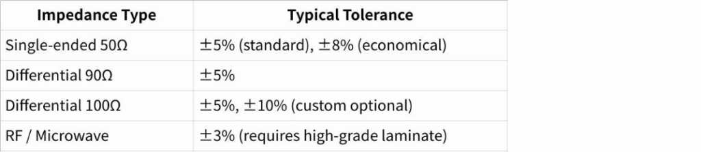
点击图片可查看完整电子表格
High-Speed Applications That Require Tight Impedance Control
PCBasic’s impedance-controlled manufacturing is widely used in:
- 5G base stations and RF front-ends
- Wi-Fi 6/6E/7 network devices
- DDR4/DDR5 memory interfaces
- PCIe, USB-C, HDMI, DisplayPort
- Automotive ADAS and radar modules
- Industrial sensors and communication modules
- Medical diagnostic electronics
When speed increases, tolerance shrinks—and our factory is built to meet these requirements.
Why High-Speed Designers Choose PCBasic
✓ Precision stackup design & simulation
✓ Engineering-assisted DFM for high-speed routing
✓ ±3% to ±8% impedance control depending on material
✓ TDR test available for every batch
✓ Full SMT + DIP assembly capability for high-frequency connectors
✓ One-stop PCB + PCBA manufacturing
✓ ISO, IATF, and IPC Class 3 manufacturing standards
Get High-Speed PCB & PCBA Manufacturing from PCBasic
Whether you are designing RF circuits, multilayer HDI boards, or high-speed digital systems, PCBasic provides accurate impedance-controlled fabrication and reliable PCB assembly support. With robust engineering, strict processing control, and advanced TDR testing, we ensure your signals reach their destination cleanly and reliably.
Ready to build your high-speed board?
Visit PCBasic and request an instant quote today.
Also Read-The best tech trends for small businesses in 2024